Materials Science and Engineering/List of Topics
< Materials Science and EngineeringIntroduction to Solid State Chemistry
Lecture 1
- Taxonomy of Chemical Species
- Origins of Modern Chemistry
Lecture 2
- Classification Schemes of the Elements
- Mendeleyev and the Periodic Table
- Atomic Structure
Lecture 3
Lecture 4
- Atomic Spectra of Hydrogen
- Matter-Energy Interactions Involving Atomic Hydrogen
Lecture 5
- The Shell Model (Bohr-Sommerfeld Model) and Multi-electron Atoms
- Quantum Numbers: n, l, m, s
Lecture 6
- De Broglie, Heisenberg, and Schrodinger
- The Aufbau Principle
- Pauli Exlusion Principle
- Hund's Rules
- Photoelectron Spectroscopy
- Average Valence Electron Energy
Lecture 7
- Octet Stability by Electron Transfer: Ionic Bonding
- Properties of Ionic Compounds: Crystal Lattice Energy
Lecture 8
- Born-Haber Cycle
- Octet Stability by Electron Sharing
- Covalent Bonding
- Lewis Structures
- Hybridization
Lecture 9
- Electronegativity
- Partial Charge
- Polar Bonds and Polar Molecules
- Ionic Character and Covalent Bonds
- Pauling's Calculation of Heteronuclear Bond Energies
Lecture 10
- LCAO MO
- Energy Level Diagrams of H2, He2, Li2
- Hybridization
- Double Bonds and Triple Bonds
- Paramagnetism and Diamagnetism
Lecture 11
- The Shapes of Molecules
- Electron Domain Theory
- Secondary Bonding
Lecture 12
- Metallic Bonding
- Band Theory of Solids (Heitler and London)
- Band Gaps in Metals
- Semiconductors
- Insulators
- Absorption Edge of a Semiconductor
Lecture 13
- Intrinsic and Extrinsic Semiconductors
- Doping
- Compound Semiconductors
- Molten Semiconductors
Lecture 14
- Introduction to the Solid State
- The Seven Crystal Systems
- The Fourteen Bravais Lattices
Lecture 15
- Simple Cubic
- Face-Centered Cubic
- Body-Centered Cubic
- Diamond Cubic
- Crystal Coordinate Systems
- Miller Indices
Lecture 16
- Characterization of Atomic Structure
- The Generation of X-Rays and Moseley's Law
Lecture 17
- X-Ray Spectra
- Bragg's Law
Lecture 18
- X-Ray Diffraction of Crystals
- Diffractometry
- Debye-Scherrer
- Laue
- Crystal Symmetry
Lecture 19
- Defects in Crystals
- Point Defects
- Line Defects
- Interfacial Defects
- Voids
Lecture 20
- Amorphous Solids
- Glass Formation
- Inorganic Glasses
- Silicates
Lecture 21
- Engineered Glasses
- Network Formers
- Network Modifiers
- Intermediates
- Properties of Silicate Glasses
- Metallic Glass
Lecture 22
- Chemical Kinetics
- The Rate Equation
- Order of Reaction
- Rate Laws of Zeroth, First, and Second Order Reactions
- Temperature Dependence of Rate of Reaction
Lecture 23
- Fick's First Law and Steady-state Diffusion
- Dependence of the Diffusion Coefficient on Temperature and on Atomic *Arrangement
Lecture 24
- Fick's Second Law (FSL)
- Transient-State Diffusion
- Error Function Solutions to FSL
Lecture 25
- Solutions
- Solute
- Solvent
- Solubility Rules
- Solubility Producet
Lecture 26
- Acids and Bases
- Arrhenius
- Bronsted-Lowry
- Lewis Definition
- Acid Strength and pH
Lecture 27
- Basic Concepts of Organic Chemistry
- Alkanes
- Alkenes
- Alkynes
- Aromatics
- Functional Groups
- Alcohols and Ethers Aldehydes and Ketones
- Esters
- Amines
Lecture 28
- Organic Glasses - Polymers
- Synthesis by Addition Polymerization and by Condensation *Polymerization
Lecture 29
- Structure-Property Relationship in Polymers
- Crystalline Polymers
Lecture 30
- Biochemisty
- The Amino Acids
- Peptides
- Proteins
Lecture 31
- Protein Structure
- Primary
- Secondary
- Tertiary
- Denaturing of Proteins
Lecture 32
- Ipids: Self Assembly into Bilayers
- Nucleic Acids
- DNA
- Encoding Information of Protein Synthesis
- Electrochemistry of Batteries and Fuel Cells
Lecture 34
Two-Component Phase Diagrams: Limited Solid Solubility Lever Rule
Quantum Mechanics
- Origins of Quantum Physics
- Postulates and Mathematical Formalism of Quantum Mechanics
- Mathematical Tools of Quantum Mechanics
- The Schrodinger Equation
- One-Dimensional Arrangements
- Angular Momentum
- Three-Dimensional Arrangements
- Rotations and Addition of Angular Momentum
- Identical Particles
- Approximation Methods of Stationary States
- Time-Dependent Pertubation Theory
Materials
- Structure of Crystalline Solids
- Imperfections in Solids
- Phase Diagrams
- Phase Transformations
- Metal Alloys
- Structures and Properties of Ceramics
- Structures and Properties of Ceramics
- Applications and Processing of Ceramics
- Polymer Structures
- Characteristics, Applications, and Processing of Polymers
- Composites
- Corrosion and Degradation of Materials
Thermodynamics
- Zeroth Law of Thermodynamics
- Equations of State
- First Law of Thermodynamics
- Second Law of Thermodynamics
- Third Law of Thermodynamics
- Chemical Equilibrium
- Phase Equilibrium
- Electrochemical Equilibrium
- Ionic Equilibria
Statistical Mechanics
Probability
Classical Statistical Mechanics
- Clasical Mechanics
- Equations of Motion
- Langrangian Formulation
- Microscopic State of a System
- Equilibrium Ensembles
Quantum Statistical Mechanics
- Vibrations of a Solid
Kinetics
- Introduction
- Irreversible Thermodynamics
- Driving Forces and Fluxes for Diffusion
- Self-Diffusion and Interdiffusion
- Diffusion Potential
- The Diffusion Equation
- Diffusion in Crystals
- Diffusion in Noncrystalline Materials
- Surface Evolution Due to Capillary Forces
- Surface Evolution Due to Capillary Forces
- Particle Coarsening
- Grain Growth
- Anisotropic Surface, Diffusional Creep, and Sintering
- General Features of Phase Transformations
- Spinodal Decomposition and Continuous Ordering
- Nucleation
- Diffusional Growth
- Morphological Stability of Moving Interfaces
- Kinetics of Nucleation and Growth Transformations
Mechanics of Materials
- Introduction to Elasticity
- Tensors
- Stress and Strain
- Generalized Hooke's Law
- Physical Origin of Elastic Moduli
- Composites
- Cellular Solids
- Viscoelasticity
- Continuum Plasticity
- Dislocation Mechanics
- Mechanism of Low Temperature Plasticity
- Continuum Creep Response
- Mechanisms of Creep Deformation
Electronic Properties of Engineering Materials
Conductors and Resistors
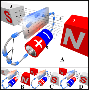
Hall effect diagram, showing electron flow (rather than conventional current).
Legend:
1. Electrons (not conventional current!)
2. Hall element, or Hall sensor
3. Magnets
4. Magnetic field
5. Power source
Description:
In drawing "A", the Hall element takes on a negative charge at the top edge (symbolised by the blue color) and positive at the lower edge (red color). In "B" and "C", either the electric current or the magnetic field is reversed, causing the polarization to reverse. Reversing both current and magnetic field (drawing "D") causes the Hall element to again assume a negative charge at the upper edge.
- Ohm's Law
- Ohm's law states that, in an electrical circuit, the current passing through a conductor between two points is directly proportional to the potential difference (i.e. voltage drop or voltage) across the two points, and inversely proportional to the resistance between them.
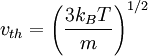
- Average kinetic energy:

- Average thermal velocity:
- Charge carrier density:


- Conductivity:

- Acceleration:

- Average drift velocity of the free-electron gas is the acceleration times the average time between collisions:

- Conductivity:

- Average kinetic energy:
- Ohm's law states that, in an electrical circuit, the current passing through a conductor between two points is directly proportional to the potential difference (i.e. voltage drop or voltage) across the two points, and inversely proportional to the resistance between them.
- Drude Model
- The Drude model of electrical conduction was developed in the 1900s by Paul Drude to explain the transport properties of electrons in materials (especially metals). The Drude model is the application of kinetic theory to electrons in a solid. It assumes that the material contains immobile positive ions and an "electron gas" of classical, non-interacting electrons of density n, each of whose motion is damped by a frictional force due to collisions of the electrons with the ions, characterized by a relaxation time τ.
- Resistance Modeled as Viscosity
- Hall Effect
- The Hall effect refers to the potential difference (Hall voltage) on the opposite sides of an electrical conductor through which an electric current is flowing, created by a magnetic field applied perpendicular to the current.
- A particle of charge
 moving with a velocity
  in a magnetic field
  experiences force:
  n
n - AC/DC
- An alternating current (AC) is an electrical current whose magnitude and direction vary cyclically, as opposed to direct current, whose direction remains constant. The usual waveform of an AC power circuit is a sine wave, as this results in the most efficient transmission of energy. However in certain applications different waveforms are used, such as triangular or square waves. Used generically, AC refers to the form in which electricity is delivered to businesses and residences. However, audio and radio signals carried on electrical wire are also examples of alternating current. In these applications, an important goal is often the recovery of information encoded (or modulated) onto the AC signal.
- Heat Conductivity
- In physics, thermal conductivity, k, is the property of a material that indicates its ability to conduct heat. It is used primarily in Fourier's Law for heat conduction.
- Heat Capacity
- Heat capacity (symbol: Cp) — as distinct from specific heat capacity — is the measure of the heat energy required to increase the temperature of an object by a certain temperature interval. Heat capacity is an extensive property because its value is proportional to the amount of material in the object; for example, a bathtub of water has a greater heat capacity than a cup of water.
Optical Properties of Conductors
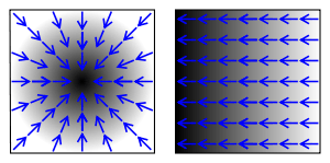
In the above two images, the scalar field is in black and white, black representing higher values, and its corresponding gradient is represented by blue arrows.
- Del operator
- In vector calculus, del is a vector differential operator represented by the nabla symbol:
 . Del is a mathematical tool serving primarily as a convention for mathematical notation; it makes many equations easier to comprehend, write, and remember. Depending on the way del is applied, it can describe the gradient (slope), divergence (degree to which something converges or diverges) or curl (rotational motion at points in a fluid). More intuitive descriptions of each of the many operations del performs can be found below.
- In vector calculus, del is a vector differential operator represented by the nabla symbol:
- Gradient
- In vector calculus, the gradient of a scalar field is a vector field which points in the direction of the greatest rate of increase of the scalar field, and whose magnitude is the greatest rate of change.
- Divergence
- In vector calculus, the divergence is an operator that measures the magnitude of a vector field's source or sink at a given point; the divergence of a vector field is a (signed) scalar. For a vector field that denotes the velocity of air expanding as it is heated, the divergence of the velocity field would have a positive value because the air expands. If the air cools and contracts, the divergence is negative. The divergence could be thought of as a measure of the change in density.
- Curl
- In vector calculus, curl is a vector operator that shows a vector field's "rate of rotation", that is the direction of the axis of rotation and the magnitude of the rotation. It can also be described as the circulation density. In many European countries the operator is called rot (short for rotor) instead of curl.
- Permittivity
- Permittivity is a physical quantity that describes how an electric field affects and is affected by a dielectric medium, and is determined by the ability of a material to polarize in response to the field, and thereby reduce the total electric field inside the material. Thus, permittivity relates to a material's ability to transmit (or "permit") an electric field. It is directly related to electric susceptibility. For example, in a capacitor, an increased permittivity allows the same charge to be stored with a smaller electric field (and thus a smaller voltage), leading to an increased capacitance.
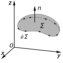
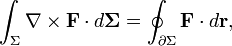
An illustration of Kelvin-Stokes theorem with surface  its boundary
  and orientation
its boundary and orientation - Stoke's Theorem
- Stokes' theorem (or Stokes's theorem) in differential geometry is a statement about the integration of differential forms which generalizes several theorems from vector calculus. It is named after Sir George Gabriel Stokes (1819–1903), although the first known statement of the theorem is by William Thomson (Lord Kelvin) and appears in a letter of his to Stokes.
- The classical Kelvin-Stokes theorem:
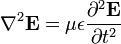
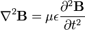
- Derivation of the Wave Equation with Maxwell's Equations
- The wave equation is an important second-order linear partial differential equation that describes the propagation of a variety of waves, such as sound waves, light waves and water waves. It arises in fields such as acoustics, electromagnetics, and fluid dynamics. Historically, the problem of a vibrating string such as that of a musical instrument was studied by Jean le Rond d'Alembert, Leonhard Euler, Daniel Bernoulli, and Joseph-Louis Lagrange.
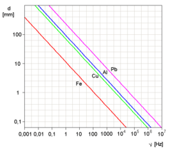
Skin depths for some metals
- Skin Depth
- When an electromagnetic wave interacts with a conductive material, mobile charges within the material are made to oscillate back and forth with the same frequency as the impinging fields. The movement of these charges, usually electrons, constitutes an alternating electric current, the magnitude of which is greatest at the conductor's surface. The decline in current density versus depth is known as the skin effect and the skin depth is a measure of the distance over which the current falls to 1/e of its original value. A gradual change in phase accompanies the change in magnitude, so that, at a given time and at appropriate depths, the current can be flowing in the opposite direction to that at the surface.
- Ionosphere
- The ionosphere is the uppermost part of the atmosphere, distinguished because it is ionized by solar radiation. It plays an important part in atmospheric electricity and forms the inner edge of the magnetosphere. It has practical importance because, among other functions, it influences radio propagation to distant places on the Earth. It is located in the Thermosphere.
- Effective Mass
- In solid state physics, a particle's effective mass is the mass it seems to carry in the semiclassical model of transport in a crystal. It can be shown that, under most conditions, electrons and holes in a crystal respond to electric and magnetic fields almost as if they were free particles in a vacuum, but with a different mass. This mass is usually stated in units of the ordinary mass of an electron me (9.11×10⁻³¹ kg).
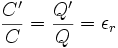
Insulators and Capacitors
- Polarization:
- In classical electromagnetism, the polarization density (or electric polarization, or simply polarization) is the vector field that expresses the density of permanent or induced electric dipole moments in a dielectric material. The polarization vector P is defined as the dipole moment per unit volume. The SI unit of measure is coulombs per square metre.
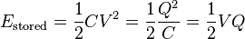
- Capacitor:
- A capacitor is an electrical/electronic device that can store energy in the electric field between a pair of conductors (called "plates"). The process of storing energy in the capacitor is known as "charging", and involves electric charges of equal magnitude, but opposite polarity, building up on each plate. The capacitor's capacitance (C) is a measure of the amount of charge (Q) stored on each plate for a given potential difference or voltage (V) which appears between the plates:

- Dielectric constant:
- The relative static permittivity (or static relative permittivity) of a material under given conditions is a measure of the extent to which it concentrates electrostatic lines of flux. It is the ratio of the amount of stored electrical energy when a potential is applied, relative to the permittivity of a vacuum. The relative static permittivity is the same as the relative permittivity evaluated for a frequency of zero.
- Electric displacement:
- In physics, the electric displacement field or electric induction is a vector field \mathbf{D} that appears in Maxwell's equations. It accounts for the effects of unbound charges within materials. "D" stands for "displacement," as in the related concept of displacement current in dielectrics.
- Electronic polarizability:
- The theoretical dielectric strength of a material is an intrinsic property of the bulk material and is dependent on the configuration of the material or the electrodes with which the field is applied. At breakdown, the electric field frees bound electrons. If the applied electric field is sufficiently high, free electrons may become accelerated to velocities that can liberate additional electrons during collisions with neutral atoms or molecules in a process called avalanche breakdown. Breakdown occurs quite abruptly (typically in nanoseconds), resulting in the formation of an electrically conductive path and a disruptive discharge through the material. For solid materials, a breakdown event severely degrades, or even destroys, its insulating capability.
- Dielectric strength:
- The theoretical dielectric strength of a material is an intrinsic property of the bulk material and is dependent on the configuration of the material or the electrodes with which the field is applied. At breakdown, the electric field frees bound electrons. If the applied electric field is sufficiently high, free electrons may become accelerated to velocities that can liberate additional electrons during collisions with neutral atoms or molecules in a process called avalanche breakdown. Breakdown occurs quite abruptly (typically in nanoseconds)., resulting in the formation of an electrically conductive path and a disruptive discharge through the material. For solid materials, a breakdown event severely degrades, or even destroys, its insulating capability. Dielectric strength (MV/m) of various common materials:
| Substance | Dielectric Strength (MV/m) |
|---|---|
| Air | 3 |
| Quartz | 8 |
| Strontium titanate | 8 |
| Neoprene rubber | 12 |
| Nylon | 14 |
| Pyrex glass | 14 |
| Silicone oil | 15 |
| Paper | 16 |
| Bakelite | 24 |
| Polystyrene | 24 |
| Teflon | 60 |
Optical Properties of Insulators
- Wave equations in a dielectric
- Relationship between dielectric constant and index of refraction


- Snell's law
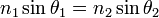
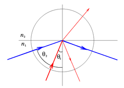
The larger the angle to the normal, the smaller is the fraction of light transmitted, until the angle when total internal reflection occurs. (The colour of the rays is to help distinguish the rays, and is not meant to indicate any colour dependence.)
- Total internal reflection
- Total internal reflection is an optical phenomenon that occurs when a ray of light strikes a medium boundary at an angle larger than the critical angle with respect to the normal to the surface. If the refractive index is lower on the other side of the boundary no light can pass through, so effectively all of the light is reflected. The critical angle is the angle of incidence above which the total internal reflection occurs.
- Dispersion
- In optics, dispersion is the phenomenon that the phase velocity of a wave depends on its frequency. In a prism, dispersion causes the spatial separation of a white light into spectral components of different wavelengths. Dispersion is most often described in light waves, but it may happen to any kind of wave that interacts with a medium or can be confined to a waveguide, such as sound waves. Dispersion is sometimes called chromatic dispersion to emphasize its wavelength-dependent nature.
- Attenuation
- Attenuation is the reduction in amplitude and intensity of a signal. Signals may be attenuated exponentially by transmission through a medium, in which case attenuation is usually reported in dB with respect to distance traveled through the medium. Attenuation can also be understood to be the opposite of amplification. Attenuation is an important property in telecommunications and ultrasound applications because of its importance in determining signal strength as a function of distance. Attenuation is usually measured in units of decibels per unit length of medium (dB/cm, dB/km, etc) and is represented by the attenuation coefficient of the medium in question. Attenuation decreases the intensity of electromagnetic radiation due to absorption or scattering of photons. Attenuation does not include the decrease in intensity due to inverse-square law geometric spreading. Therefore, calculation of the total change in intensity involves both the inverse-square law and an estimation of attenuation over the path.
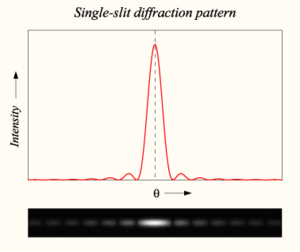
Graph and image of single-slit diffraction
- Diffraction
- Diffraction refers to various phenomena associated with the bending of waves when they interact with obstacles in their path. It occurs with any type of wave, including sound waves, water waves, and electromagnetic waves such as visible light, x-rays and radio waves. As physical objects have wave-like properties, diffraction also occurs with matter and can be studied according to the principles of quantum mechanics. While diffraction always occurs when propagating waves encounter obstacles in their paths, its effects are generally most pronounced for waves where the wavelength is on the order of the size of the diffracting objects. The complex patterns resulting from the intensity of a diffracted wave are a result of interference between different parts of a wave that traveled to the observer by different paths.
This article is issued from Wikiversity - version of the Sunday, September 06, 2015. The text is available under the Creative Commons Attribution/Share Alike but additional terms may apply for the media files.