Semiconductors/Transistors as Switches
< Semiconductors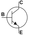
A transistor is the most basic of digital devices. It has three terminals: the base, the collector, and the emitter. These terminals are connected to a piece of silicon that has been treated to have certain properties that allow it to behave as an amplifier, a switch, or other electronic devices.
Transistors as a Digital Device
At the most basic level, a transistor can be thought of as a switch, allowing current to flow if the base of the transistor is fed a reasonably high voltage compared to the emitter. This means that in a five volt system (+5v), voltages between 0v and 1v are considered 'low' and voltages between 4v and 5v are considered 'high'. Voltages between 1v and 4v are considered undefined and should not be applied to the input of a transistor acting as a logic device. Because transistors do not act like an ideal switch, they are arranged in ways that allow them to more closely emulate an ideal logic gate. More information on the different types of transistor families and associated logic will come later.
Transistor Anatomy
There are two main types of transistors: Bipolar Junction (BJT) and Metal-Oxide Semiconductor (MOS). These transistors are fabricated differently from slightly different materials, however they can be arranged to perform similar functions.
Inside a BJT
A Bipolar Junction Transistor is made up of a piece of silicon that has been treated to create a 'channel' in the silicon. First, an undoped (untreated) piece of silicon is selected. (Undoped silicon acts as an insulator, preventing the flow of current.) Next, a process is used to create an N-type channel in the silicon. This is silicon that has an overabundance of negative charge carriers (electrons). A second channel is created in the first, this time with P-type silicon. P-type silicon carries current because of the overabundance of positive charge carriers ('holes', they're called). The process has created three regions in the silicon, an N-type region, a P-type region, and another N-type region. The base terminal is connected to the P-type region, while the collector and emitter are connected to the opposing N-type regions.
Effectively, for the average transistor, when the base of the transistor rises above 0.7V (compared to the emitter), the impedance between the collector and the emitter begins to fall, until at about 1.2V it has virtually no resistance.
BJTs are current controlled devices.
The following assumes that the BJT is NPN construction. It is possible to construct BJTs as PNP but these are normally slower and thus not popular.
The base emitter junction is a diode. If the device is based on silicon (as opposed to germanium or 3-5 compoundes like galium/arsnides) then the forward volt drop of the diode is assumed to be 0.7V.
In practice the transistor starts to change state at 0.65V and by 0.75V is fully saturated. This means that the electric current flowing from collector to emitter is near 0 whilst the base emitter voltage is below 0.65V (and hence there is no electric current flowing from base to emitter) then there is no current flow from collector to emitter.
As the voltage from base to emitter is raised to 0.75 the current flow from base to emitter will increase by at least a factor of 100. This will increase the flow of current from collector to base by at least the same amount.
By the time the base to emitter voltage is greater than 0.75V the current flowing from collector to emitter will typically be 100 times greater (this is amplification) and the collector to emitter voltage will have droped to 0.3V and cannot be further reduced hence the transistor will be said to be in saturation.
Technically the transistor is saturated when the collector voltage is below the base voltage.
An example
Reference: "Transistor Manual" published in 1964 by General Electric Company
Page 44 has two graphs related to the NPN Transistor 2N1613, whose tabulated data are shown on page 548.
- a) The Volt-Current (VI) characteristic (Collector current versus collector-to-base voltage) for different base currents), and
- b) The base current versus base-to-emitter voltage.
The VI graph shows that
- negligible collector current flows if the base current is zero,
- about 9 mA flows if the base current is roughly 0.1 mA,
- about 45 mA flows if the base current is roughly 0.4 mA,
- about 75 mA flows if the base current is roughly 0.7 mA.
- A change of base current from 0.1 to 0.4, of 0.3 mA, results in a collector current change from 9 to 45, of 36 mA, so that the approximate current gain is 36 divided by 0.3 = 120.
- A change of base current from 0.4 to 0.7 mA, of 0.3 mA, results in a collector current change from 45 to 75, of 30 mA, so that the approximate current gain (current amplification) is (30 divided by 0.3 =) 100.
- MAXIMUM collector to base voltage, per data sheet, is 60 V, but the VI graph only shows voltage up to 50, which is below the permitted maximum.
- The graph for the base VI relationship shows that there is negligible base current if the base to emitter voltage is below 0.5 V.
- It also shows that for a base current of 5 mA to flow only about 0.9 V from base to emitter is needed. From above, only up to about 0.7 mA base current are needed.
- From the data sheet we see that the rated maximum power for this transistor is only 0.8 Watt if the case temperature in free air cooling is no more than 25 degrees Celsius, but that a maximum of 1.7 Watts would result in a very hot case temperature of about 100 degrees C. Let us use only up to 0.8 Watts; this power curve is not shown on the collector current graph, but we can add it there: For 0.8 Watts and a collector current of 100 mA the collector-emitter voltage is (0.8 W divided by 0.1 A =) 8V, 90 mA and 8.9V, 80 mA and 10V, ...... 45V and 18 mA, 50V and 16 mA.
- Assume we have two resistors in series connected to the power supply, and that one of these resistors is variable, the other one is fixed. As we vary the variable resistor from zero Ohms to its maximum, the voltage across it varies too. Obviously if it is zero resistance then the voltage across it is also zero, and the current is a maximum, being the voltage of the power supply divided by only the fixed resistor. If we set the variable resistor to its maximum value then the current is the power supply voltage divided by the sum of the two resistor values, and the voltage across the variable resistor is its resistance times the power supply voltage divided by the sum of the values in Ohms of these 2 resistors. Think of the variable resistor being the transistor, it being connected to the power supply via a fixed resistor. We can show on the collector current versus voltage graph a straight line for any such resistor, and we choose a line that is still within the permitted power area, possibly approximately a tangent to the maximum power curve. The graph in the book shows such a line, called a load line, connecting the 0V, 80 mA point with the 45V, 0 mA point. It indicates that the power supply voltage is 45V (zero current), and that the load resistor passes 80 mA if full power supply voltage is across it. Therefore the value of that load resistance is (45V divided by 0.08 A =) 562.5 Ohms. The nearest standard size resistor is 560 Ohms, to be connected between the power supply and the transistor.
- The collector graph shows also that as the base current is varied as above, there is a corresponding voltage change across the transistor, with the voltage change across the resistor being the difference between the voltage of the power supply and the voltage at the collector. Note that this voltage change is much higher than the voltage change in the base circuit; voltage amplification results.