Semiconductors/MESFET Transistors
< SemiconductorsMESFET Operation
Assume an N channel MESFET with uniform doping and sharp depletion region shown in figure 1.
The depletion region  is given by the depletion width for a
diode. Where the voltage is the voltage from the gate to the
channel, where the channel voltage is given for a position x along
the channel as
is given by the depletion width for a
diode. Where the voltage is the voltage from the gate to the
channel, where the channel voltage is given for a position x along
the channel as  .
.
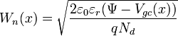
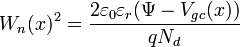
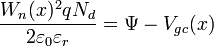
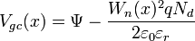
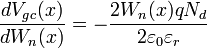 (1)
(1)
The current density in the channel is given by:

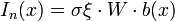
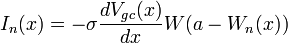
where:
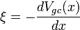
Therefore,
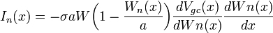

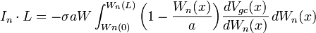
Substituting from equation 1:

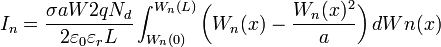
![I_n= \frac{2\sigma aWqN_d}{2\varepsilon_0\varepsilon_rL}
\bigg[\frac{W_n^2(x)}{2}-\frac{W_n^3(x)}{3a}\bigg]_{W_n(0)}^{W_n(L)}](../I/m/b9608201851bc115f129f46959339ec5.png)
![I_n= \frac{2\sigma aWqN_d}{2\varepsilon_0\varepsilon_rL}
\bigg[\frac{W_n^2(L)-W_n^2(0)}{2}-\frac{W_n^3(L)-W_n^3(0)}{3a}\bigg]](../I/m/8f9665055b98e069a5c28dc74ef0a535.png)
![I_n= \frac{2\sigma aWqN_da^2}{6L\cdot
2\varepsilon_0\varepsilon_r}
\bigg[\frac{3(W_n^2(L)-W_n^2(0))}{a^2}-\frac{2(W_n^3(L)-W_n^3(0))}{a^3}\bigg]](../I/m/dd07ee209d84ccd1409f7222892f29ee.png)
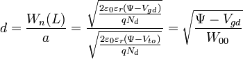
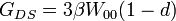
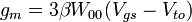
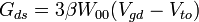
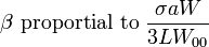
One defines constant Β as the channel conductance with no depletion. And the work function to deplete the channel W00 [1]:
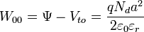

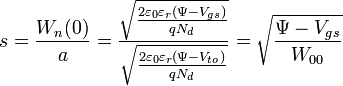
We now define Vto, the voltage such that the channel is pinched off. d is the ratio of channel depletion to maximum depletion for the drain. s the ratio of channel depletion to maximum depletion for the source.
Substituting:
![I_n= W\cdot \frac{\sigma a\cdot W_{00}}{3L}
\big[3(d^2-s^2)-2(d^3-s^3)\big]](../I/m/ce6c5557c43a03680039426f00070383.png)
![I_n= W \cdot\beta W_{00}^2 \big[3(d^2-s^2)-2(d^3-s^3)\big]](../I/m/59162db82488b009a637b52c22fc54af.png) (2)
(2)
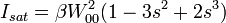
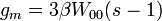
Equation 2 is Shockley's expression [2] for drain current in the linear region. When the device enters saturation, one end is pinched off(normally the drain). Thus $d=1$ and one may derive the equation for the saturation region:
Simpler Model
![I_{ds}=\frac{3}{2}\beta
W_{00}^2\bigg[\frac{(V_{gs}-v_{to})^2}{W_{00}^2}-\frac{(V_{gd}-v_{to})^2}{W_{00}^2}\bigg]](../I/m/8f43a0f80f02e6e26af7ec8869424536.png)
General power law:
It was found that a general power law provided a better fit for real devices [3].
![I_{ds}=\beta\big[(V_{gs}-V_{to})^Q-(V_{gd}-V_{to})^Q\big]](../I/m/6da5048715665150ada14b640580b357.png)
Where Q is dependent on the doping profile and a good fit is usually obtained for Q between 1.5 and 3. A general power law is approximately equal to Shockley's equation for Q = 2.4. Β is also empirically chosen and is proportion to the previous Β
Modelling the various regions is done though model binning. This however infers that a sharp transition exists from one region to another, which may not be accurate.
![I_{ds}=\left\{
\begin{matrix}
0&V_{gs}<V_{to}\\
\beta\big[(V_{gs}-V_{to})^Q-(V_{gd}-V_{to})^Q\big]&V_{gs}\le
V_{gd}\\
\beta(V_{gs}-V_{to})^Q & V_{gs}>V_{gd}
\end{matrix}\right.](../I/m/3b8051e1cb04dd4a0d1301bccd499e83.png)
References
[1] A. E. Parker. Design System for Locally Fabricated Gallium Arsenide Digital Integrated Circuits. PhD thesis, Sydney University, 1990.
[2] W. Shockley. A unipolar field-effect transistor. IEEE Trans/ Electron Devices, 20(11):1365–1376, November 1952.
[3] I. Richer and R.D. Middlebrook. Power-law nature of field-effect transistor experimental characteristics. Proc. IEEE, 51(8):1145–1146, August 1963.