Nanotechnology/Scanning probe microscopy
< Nanotechnology| Navigate |
|---|
| << Prev: Electron Microscopy |
| >< Main: Nanotechnology |
| >> Next: Additional Methods |
|
|
| Section on AFM |
| Section on STM |
| Section on SNOM |
Scanning probe microscopy
Scanning probe microscopy covers the methods where a sharp tip is scanned over a surface in a raster pattern and the interaction with the surface is recorded in each pixel to form an image of the interaction. There are a multitude of methods and interactions in SPM. Broadly speaking, there are three main categories:
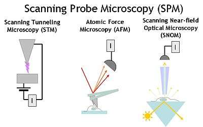
Overview of the main types of Scanning Probe Microscope types:
Scanning Tunneling Microscope (STM) - using the tunneling current I between the outermost atom of a conducting probe within an atomic distance from a substrate to map out the sample topography and electrical properties.
Atomic Force Microscope (AFM) - using the van der Waals forces or contact forces between a tip and the sample to measure the sample topography or mechanical properties.
Scanning Near-field Optical Microscope (SNOM) - using the scattered light through a sub-wavelength aperture to form an image.
- In scanning tunneling microscopy (STM), one uses an atomically sharp metallic tip and records the minute tunneling current between the tip and the surface, when the tip is hovering so close to the surface that electrons can move between the surface and the tip.
- In Atomic force microscopy (AFM), a cantilever with a sharp tip - somewhat like the needle of an old record player - is scanned over the surface and the topography or surface softness can be recorded.
- In Scanning near-field optical microscopy (SNOM) a probe with a smalle aperture is scanned over the surface collecting the light comming from regions much smaller than the wavelength of the light used.
Atomic force microscope (AFM)
- Atomic force microscope (AFM)
- Kelvin force microscopy
- Magnetic force microscope
- Scanning voltage microscopy
- Magnetic resonance force microscope
- Lateral force microscopy
Scanning tunneling microscopy (STM)
Scanning Near-field optical microscopy (SNOM)
Wiki links:
Resources
- A Practical Guide to Scanning Probe Microscopy by Rebecca Howland and Lisa Benatar
- homebrew atomic-resolution microscope
References
See also notes on editing this book about how to add references Nanotechnology/About#How_to_contribute.
This article is issued from Wikibooks. The text is licensed under Creative Commons - Attribution - Sharealike. Additional terms may apply for the media files.