Microprocessor Design/Wire Wrap
< Microprocessor DesignHistorically, most of the early CPUs were built by attaching integrated circuits (ICs) to circuit boards and wiring them up.
Nowadays, it's much faster to design and implement a new CPU in a FPGA -- the result will probably run faster and use less power than anything spread out over multiple ICs.
However, some people still design and build CPUs the old-fashioned way. Such a CPU is sometimes called a "home brew CPU" or a "home built CPU".
Some people feel that physically constructing a CPU in this way, since it allows students to probe the inner workings of the CPU, it helps them "Touch the magic"[1], helps them learn and understand the underlying electronics and hardware.
Overview
A homebrew CPU is a central processing unit constructed using a number of simple integrated circuits, usually from the 7400 Series. When planning such a CPU, the designer must not only consider the hardware of the device but also the instructions the CPU will have, how they will operate, the bit patterns for each one, and their mnemonics. Before the existence of computer based circuit simulation, many commercial processors from manufacturers such as Motorola were first constructed and tested using discrete logic. Those commercial processors include the Motorola 6800,[2] the Motorola 6809,[3] and the Hewlett-Packard PA-RISC TS1.[4]
Although no limit exists on data bus sizes when constructing such a CPU, the number of components required to complete a design increases exponentially as bus size gets wider. Common physical data bus sizes are 1-bit, 4-bits, 8-bits, and 16-bits. Incomplete design documents exist for a 40-bit CPU.[5] A microcoded CPU may be able to present a significantly different instruction set to the application programmer than seems to be directly supported by the hardware used to implement it. For example, the 68000 presented a 32-bit instruction set to the application programmer -- a 32-bit "add" was a single instruction -- even though internally it was implemented with 16-bit ALUs. For example, the Zilog Z80, one of the most commonly used CPU families of all time,[6] presented an 8-bit instruction set to the application programmer -- even though internally it was implemented with a single 4-bit ALU.[7]
For example, w:serial computers, even though they do calculations one bit per clock cycle, present a instruction set that deals with much wider words -- often 12 bits (PDP-8/S; PDP-14), 24 bits (D-17B), or even wider -- 39 bits (Elliott 803).
Notable Homebrew CPUs
The Magic-1 is a CPU with an 8-bit data bus and 16-bit address bus running at about 3.75MHz 4.09 Mhz.
The Mark I FORTH also has a 8-bit data bus and 16-bit address bus, but runs at 1MHz.
The V1648CPU is a CPU with a 16-bit data bus and 48-bit address bus that is currently being designed.
APOLLO181 is a homemade didactic 4-bit processor made of TTL logics and bipolar memories, based upon the Bugbook® I and II chips, in particular on the 74181 (by Gianluca.G, Italy, May 2012).
Parts
...
chips
bus
Practically all CPU designs include several 3-state buses -- an "address bus", a "data bus", and various internal buses.
A 3-state bus is functionally the same as a multiplexer. However, there is no physical part you can point to and say "that is the multiplexer" in a 3-state bus; it's a pattern of activity shared among many parts. The only reason to use a 3-state bus is when it requires fewer chips or fewer, shorter wires, compared to an equivalent multiplexer arrangement. When you want to select between very few pieces of data that are close together, and most of that data is stored on a chip that only has 2-state outputs, it may require fewer chips and less wiring to use actual multiplexer chips. When you want to select between many pieces of data (one of many registers, or one of many memory chips, etc.), or many of the chips holding that data already have 3-state outputs, it usually requires fewer chips to use a 3-state bus (even counting the "extra" 3-state buffer between the bus and each thing that doesn't already have 3-state outputs).
A typical register file connected to a 3-state 16-bit bus on a TTL CPU includes:
- octal 2-state output registers (such as 74x273), 2 chips per 16-bit register
- octal 3-state non-inverting buffers (such as 74x241), 2 chips per 16-bit register per bus
- a demultiplexer with N inputs (driven by microcode) and 2^N output wires that select the 3-state buffers of one of up to 2^N possible things that can drive the bus, 1 chip per bus.
Later we discuss shortcuts that may require fewer chips.
74181
Like many historically important commercial computers, many home-brew CPUs use some version of the 74181, the first complete ALU on a single chip.[8] (Versions of the 74181 include the 74F181, the 40181[citation needed], the 74AS181, the 72LS181, the 74HCT181, etc.). The 74181 is a 4-bit wide ALU can perform all the traditional add / subtract / decrement operations with or without carry, as well as AND / NAND, OR / NOR, XOR, and shift.
A typical home-brew CPU uses 4 of these 74181 chips to build an ALU that can handle 16 bits at once, like the Data General SuperNova.[9] The simplest home-brew CPUs have only one ALU, which at different times is used to increment the program counter, do arithmetic on data, do logic operations on data, and calculate addresses from base+offset.
Some people who build TTL CPUs attempt to "save chips" by building that one ALU of less than the largest word size (which is often 16 bits in TTL computers). For example, the earliest Data General Nova computers used a single 74181 and processed all data 4 bits at a time.[9] Unfortunately, this adds complexity elsewhere, and may actually increase the total number of chips needed.[10][11][12]
The simplest 16-bit TTL ALU wires the carry-out of each 74181 chip to the carry-in of the next, creating a ripple-carry adder.
Historically, some version of the look ahead carry generator 74182 was used to speed up "add" and "subtract" to be about the same speed as the other ALU operations.
Historically, some people who built TTL CPUs put two or more independent ALU blocks in a single CPU -- a general-purpose ALU for data calculations, a PC incrementer, an index register incrementer/decrementer, a base+offset address adder, etc.
We discuss ripple-carry adders, look-ahead carry generators, and their effects on other parts of a CPU at Microprocessor Design/Add and Subtract Blocks.
alternatives to 74181
Some people find that '181 chips are becoming hard to find.
Quite a few people building "TTL CPUs" use GAL chips (which can be erased and reprogrammed). [13] A single GAL20V8 chip can replace a 74181 chip.[14] Often another GAL chip can replace 2 or 3 other TTL chips.
Other people building "TTL CPUs" find it more magical to build a programmable machine entirely out of discrete non-programmable chips. Are there any reasonable alternatives to the '181 for building an ALU out of discrete chips? The Magic-1 uses 74F381s and a 74F382 ALUs;[15] is there any variant of the '381 and '382 chips that are any easier to find than a '181? ... the 74HC283, 74HCT283, MC14008 chips only add; they don't do AND, NAND, etc. ...
Many commercial machines, such as the Data General Nova 4, used four AM2901 ALUs "in parallel" to build each 16 bit ALU. Alas, these are apparently even harder to find than the 74181.
One could build the entire CPU -- including the ALU -- out of sufficient quantities of the 74153 multiplexer.[16]
One designer "built-from-scratch" a 4-bit ALU that does add, subtract, increment, decrement, "and", "or", "xor", etc. -- roughly equivalent to the 4-bit 74181 -- out of about 14 simple TTL chips: 2-input XOR, AND, OR gates.[17]
Another designer has posted a 8-bit ALU design that has more functionality than two 74181 chips -- the 74181 can't shift right -- built from 14 complex TTL chips: two 74283 4-bit adders, some 4:1 mux, and some 2:1 mux.[18]
The designers of the LM3000 CPU have proven that much of the 74181 is actually unnecessary. The 8 bit "ALU" in the LM3000 can't actually do any logical operations, only "add" and "subtract", built from two 74LS283 4-bit adders and a few other chips. Apparently those "logical" operations aren't really necessary.[19]
The MC14500B Industrial Control Unit has even less functionality than the LM3000 CPU. It is arguable that the MC14500B has close to the minimum functionality to even be considered a "CPU".[20][21] The MC14500B is perhaps the most famous "1-bit" CPU.[22][23][24][25] [26]
All of the earliest computers and most of the early massive parallel processing machines used a serial ALU, making them "1-bit CPUs".[27]
other parts
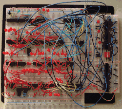
solderless breadboard approach
Solderless breadboards are perhaps the fastest way to build experimental prototypes that involve lots of changes.
For about a decade, every student taking the 6.004 class at MIT was part of a team -- each team had one semester to design and build a simple 8 bit CPU out of 7400 series integrated circuits.[28] These CPUs were built out of TTL chips plugged into several solderless breadboards connected with lots of 22 AWG (0.33 mm2) solid copper wires.[29]
wire-wrap
Traditionally, minicomputers built from TTL chips were constructed with lots of wire-wrap sockets (with long square pins) plugged into perfboard and lots of wire-wrap wire, assembled with a "wire-wrap pencil" or "wire-wrap gun".
stripboard
More recently, some "retrocomputer" builders have been using standard sockets plugged into stripboard and lots of wire-wrap wire, assembled with solder and a soldering iron.[30]
Tools
Logisim is a free logic simulator which permits digital circuits to be designed and simulated using a graphical user interface.
Design Tips
There are many ways to categorize CPUs. Each "way to categorize" represents a design question, and the various categories of that way represent various possible answers to that question that needs to be decided before the CPU implementation can be completed.
One way to categorize CPU that has a large impact on implementation is: "How many memory cycles will I hold one instruction before fetching the next instruction?"
- 0: load-instruction on every memory cycle (Harvard architecture)
- 1: At most 1 memory cycle between each load-instruction memory cycle ( load-store architecture )
- more: some instructions have 2 or more memory cycles between load-instruction memory cycles (memory-memory architecture)
Another way to categorize CPUs is "Will my control lines be controlled by a flexible microprogramming, a fixed control store, or by hard-wired control decoder that directly decodes the instruction?"
The load-store and memory-memory architectures require a "instruction register" (IR). At the end of every instruction (and after coming out of reset), the next instruction is fetched from memory[PC] and stored into the instruction register, and from then on the information in the instruction register (directly or indirectly) controls everything that goes on in the CPU until the next instruction is stored in the instruction register.
For homebrew CPUs, the 2 most popular architectures are[citation needed]:
- direct-decode Harvard architecture
- flexible microprogramming that supports the possibility of memory-memory architecture.
Another way to categorize CPUs is "How many sub-states are in a complete clock cycle?"
Many textbooks imply that a CPU has only one clock signal -- a bunch of D flip-flops each hold 1 bit of the current state of the CPU, and those flip-flops drive that state out their "Q" output. Those flip-flops always hold their internal state constant, except at the instant of the rising edge of the one and only clock, where each flip-flop briefly "glances" at their "D" input and latches the new bit, and shortly afterwards (when the new bit is different from the old bit) changes the "Q" output to the new bit.
Single clock signals are nice in theory. Alas, in practice we can never get the clock signal to every flip-flop precisely simultaneously -- there is always some clock skew (differences in propagation delay). One way to avoid these timing issues is with a series of different clock signals.[31] Another way is to use enough power[32] and carefully design a w: clock distribution network (perhaps in the form of an w: H tree) with w: timing analysis to reduce the clock skew to negligible amounts.
Relay computers are forced to use at least 2 different clock signals, because of the "contact bounce" problem.
Many chips have a single "clock input" pin, giving the illusion that they use a single clock signal -- but internally a "clock generator" circuit converts that single external clock to the multiple clock signals used by the chip.
Many historically and commercially important CPUs have many sub-states in a complete clock cycle, with two or more "non-overlapping clock signals". Most MOS ICs used dual clock signals (a two-phase clock) in the 1970s[33]
shortcuts
Building a CPU from individual chips and wires takes a person a long time. So many people take various shortcuts to reduce the amount of stuff that needs to be connected, and the amount of wiring they need to do.
- 3-state bus rather than 2-state bus often requires fewer and shorter connections.
- Rather than general-purpose registers that can be used (at different times) to drive the data bus (during STORE) or the address bus (during indexed LOAD), sometimes it requires less hardware to have separate address registers and data registers and other special-purpose registers.
- If the software guy insists on general-purpose registers that can be used (at different times) to drive the data bus (during STORE) or the address bus (during indexed LOAD), it may require less hardware to emulate them: have all programmer-visible registers drive only one internal microarchitectural bus, and (at different times) load the microarchitectural registers MAR and MDR from that internal bus, and later drive the external address bus from MAR and the external data bus from MDR. This sacrifices a little speed and requires more microcode to make it easier to build.
- Rather than 32-bit or 64-bit address and data registers, it usually requires less hardware to have 8-bit data registers (occasionally combining 2 of them to get a 16-bit address register).
- If the software guy insists on 16-bit or 32-bit or 64-bit data registers and ALU operations, it may require less hardware to emulate them: use multiple narrow micro-architectural registers to store each programmer-visible register, and feed 1 or 4 or 8 or 16 bits at a time through a narrow bus to the ALU to get the partial result each cycle, or to sub-sections of the wide MAR or MDR. This sacrifices a little speed (and adds complexity elsewhere) to make the bus easier to build. (See: 68000, as mentioned above)
- Rather than many registers, it usually requires less hardware to have fewer registers.
- If the software guy insists on many registers, it may require less hardware to emulate some of them (like some proposed MMIX implementations) or perhaps all of them (like some PDP computers): use reserved locations in RAM to store most or all programmer-visible registers, and load them as needed. This sacrifices speed to make the CPU easier to build. Alas, it seems impossible to eliminate all registers -- even if you put all programmer-visible registers in RAM, it seems that you still need a few micro-architectural registers: IR (instruction register), MAR (memory address register), MDR (memory data register), and ... what else?
- Harvard architecture usually requires less hardware than Princeton architecture. This is one of the few ways to make the CPU simpler to build *and* go faster.
Harvard architecture
The simplest kinds of CPU control logic use the Harvard architecture, rather than Princeton architecture. However, Harvard architecture requires 2 separate storage units -- the program memory and the data memory. Some Harvard architecture machines, such as "Mark's TTL microprocessor", don't even have an instruction register -- in those machines, the address in the program counter is always applied to the program memory, and the data coming out of the program memory directly controls everything that goes on in the CPU until the program counter changes. Alas, Harvard architecture makes storing new programs into the program memory a bit tricky.
microcode architecture
See Microprocessor Design/Microcodes.
Assembly Tips
...
"I don't recommend that anybody but total crazies wirewrap their own machines out of loose chips anymore, although it was a common enough thing to do in the mid- to late Seventies". -- Jeff Duntemann
Programming Tips
...
Further Reading
- ↑ "Touch the magic. By this I meant to gain a deeper understanding of how computers work" -- Bill Buzbee
- ↑ "To evaluate the 6800 architecture while the chip was being designed, Jeff's team built an equivalent circuit using 451 small scale TTL ICs on five 10 by 10 inch (25 by 25 cm) circuit boards. Later they reduced this to 114 ICs on one board by using ROMs and MSI logic devices." -- w:Motorola_6800#Development_team
- ↑ Terry Ritter and Joel Boney. "A Microprocessor for the Revolution: The 6809. Part 3: Final Thoughts". Caption on Photo 2: "The gate level TTL model of the processor involves ten boards of 80 to 120 integrated circuits each. Many of the required 10,000 connections will be wrong. The system must be tested to find and correct construction and logic errors."
- ↑ "The first implementation was the TS1, a central processing unit built from discrete transistor-transistor logic (74F TTL) devices." -- w:PA-RISC
- ↑ "Asychronous 40-bit TTL CPU" by Hans Summers 1992
- ↑ Wikipedia: Zilog Z80
- ↑ Ken Shirriff. "The Z-80 has a 4-bit ALU. Here's how it works." 2013.
- ↑ "The 74181 is a bit slice arithmetic logic unit (ALU)... The first complete ALU on a single chip ... Many computer CPUs and subsystems were based on the '181, including ... the ... PDP-11 - Most popular minicomputer of all time" -- Wikipedia:74181
- 1 2 Wikipedia: Data General Nova#Processor design
- ↑ "My Home-Built TTL Computer Processor (CPU)" by Donn Stewart
- ↑ "The basic algorithm executed by the instruction execution unit is most easily expressed if a memory address fits exactly in a word." -- "The Ultimate RISC" by Douglas W. Jones
- ↑ "it just really sucks if the largest datum you can manipulate is smaller than your address size. This means that the accumulator needs to be the same size as the PC -- 16-bits." -- "Computer Architecture"
- ↑ Andrew Holme. "Mark 2 FORTH Computer"
- ↑ GALU - A Gate Array Logic based ALU IC.
- ↑ Bill Buzbee. "Magic-1 Microarchitecture".
- ↑ Dieter Mueller. "Multiplexers: the tactical Nuke of Logic Design" 2004.
- ↑ Rodney Moffitt. Micro Programmed Arithmetic Processor. 55 TTL chips. The core 4-bit adder/subtracter has about 7 SSI chips. The ALU has about 7 additional SSI chips of logic around that core to support "and", "or", "xor", "increment", "decrement". An instruction register and a micro-programmed sequencer around the ALU handle (4-bit) "multiply" and "divide".
- ↑ Dieter Mueller. ALU with Adder. 2004.
- ↑ LM3000 CPU
- ↑ Decode Systems. "Motorola 14500B"
- ↑ "1 (Yes, ONE) bit computer? MC14500B"
- ↑ TinyMicros wiki: MC14500B
- ↑ Dennis Feucht. "Forgotten Circuits (that should be brought back): MC14500B Industrial Control Unit". EDN 2012.
- ↑ "MC14500B - a 1 bit industrial processor"
- ↑ "icu-assembler: Assembler for the Motorola MC14500B ICU written in C"
- ↑ Eric Smith. "Motorola MC14500B"
- ↑ Wikipedia: serial computer
- ↑ the VHS, a 32 bit CPU built by Kevin McCormick, Colin Bulthaup, Scott Grant and Eric Prebys for their MIT 6.004 class.
- ↑ 6.004 Contest Photos
- ↑ "Libby8" neo-retro computer by Julian Skidmore
- ↑ Bill Buzbee. Magic-1 Homebrew CPU: Clocks
- ↑ "Intel's Atom Architecture: The Journey Begins" by Anand Lal Shimpi, 2008. In a large microprocessor, the power used to drive the clock signal can be over 30% of the total power used by the entire chip.
- ↑ Wikipedia:Two-phase clock
reviews
- Everyone who builds a CPU from "real" hardware (relays, TTL chips, FPGAs, vacuum tubes, etc.) is encouraged to add their design to the home-built computers web-ring.
- Pavel Dovgalyuk. "Comparison of modern relay computers".
- Svarychevski Michail Aleksandrovich. "Homemade CPU – from scratch". Briefly compares a few notable hobbyist-built CPUs.
- other homemade CPUs
- yet more homemade CPUs
relay computers
- Harry Porter's Relay Computer (415 Relays, all identical 4PDT) ("RC1")
- "RC-3 Relay Computer" (418 relays, all identical 4PDT. 421 lights and 134 switches on its front panel. Runs at 6 Hz). RC-3 Relay Computer (background). RC-3 Relay Computer (technical details).
- "Relay Computer Two" by Jon Stanley (281 relays, of 2 types: 177 SPDT, and 104 4PDT) ("RC2")
- "Relay Binary Adder" by Jon Stanley. "a simple 4-bit relay adder with two 4-bit input storage/registers." Shows a way to build a 1-bit memory cell with 1 relay, a 1-bit half adder with 1 DPDT relay, and a 1-bit full adder with 2 relays.
- "i2 8-Bit Relay Computer" (about 300 relays, of 2 types: single-pole and double-pole, plus 2 kB static RAM for memory) by ???. The i2 instruction set is a modified version John Stanley's RC2 ISA.
- Zusie - My Relay Computer by Fredrik Andersson (uses around 330 relays, of 2 types: 4-pole and 6-pole double-throw relays, plus ~30 integrated circuits for RAM and microcode)
- relay computers by Kilian Leonhardt (in German): a "large computer" with around 1500 relays and a program EEPROM, and a "small computer" with 171 relays.
- DUO 14 PREMIUM by Jack Eisenmann (around 50 relays, including 4 addressable "crumbs" of RAM where each crumb is 2 bits, plus 48 bits of program ROM in 6x8-switch DIP switches. The only semiconductor components: 555 timer, decade counter, and transistors in the clock generator. Each command has 6 bits, and the 8 commands in the program ROM are selected by a 3-bit program counter).
- Wikipedia: Z3 (computer), designed by Konrad Zuse, the world's first working programmable, fully automatic computing machine. built with 2,000 relays.
- Z3 Nachbau, Horst Zuse's (Konrad Zuse's son) and Raul Rojas' 2001 reconstruction of the classic Z3. The 32-word, 22-bit-wide memory is also constructed entirely from relays, about 700 relays. (in German)
- Horst Zuse's new Z3 reconstruction: Created 2010 for the 100 year anniversary of Konrad Zuse's birth. About 2500 modern relays. (in German)
- Rory Mangles. Tim 7: A 4-bit relay CPU with the program stored on punch tape
- Rory Mangles. Tim 8: "one of the smallest Turing complete relay computers in the world by relay count" an 8-bit relay CPU with the program stored on punch tape, data stored in discrete capacitors (!) (no RAM chips) with one relay pole per byte; uses 152 relays, most of them single-pole.
- Pavel Dovgalyuk. A fistful of relays. Relay computer built of 4PDT relays.
discrete transistor computers
- James Newman. The Mega-processor. "put LEDs on everything so we can actually SEE the data moving and the logic happening." No integrated circuit; only LEDs and resistors and about 14,000 (?) discrete transistors (2N7000 in through-hole TO-95 package ?) in the functional part of the CPU.
- MT15 by Dieter Mueller is built almost entirely out of (around 3000) individual SMT transistors ... also has some essays on microprogramming and ALU design.
- The Q1 Computer by Joe Wingbermuehle. Built almost entirely out of (3105) individual through-hole PN2222A transistors. "Clock phases are used so that transparent latches can be used for registers to reduce transistor count at the price of speed." 8 bit data bus, 16 bit address bus.
- Svarichevsky Mikhail is apparently building a processor entirely out of discrete transistors. Using very careful analog tuning (12 resistors of various values), Svarichevsky Mikhail has developed a 4 transistor full adder: "BARSFA - 4-TRANSISTOR FULL ADDER". (Are the 4 Schottky diodes -- across the base and collector of each transistor -- really necessary, or just to improve performance?) (He also shows a canonical implementation of a CMOS full adder, requiring 28 transistors).
- Simon Inns. "4-Bit Computer" shows a 4-bit adder built entirely from AND, OR, NOT gates in turn built entirely from discrete NPN transistors and resistors. Toggle switches for the "A" and "B" 4-bit inputs; 5 LEDs to output the sum (including carry bit). (A 22 transistor full adder).
- Rory Mangles. Tiny Tim: diode-transistor logic (DTL); 400 2N3904 NPN Transistors plus diodes, resistors, capacitors, etc. gives "2700 components" (?). Has 4 registers: a Working Register (8 bit), Instruction Register (8 bit) , Address Register (12 bit), Program Counter (12 bit), and a sequencer. (Also uses some Zero Page "Registers" stored in the SRAM chip).
pneumatic computers
- "8 bit processor using logic gates made of pneumatic valves" by Minsoung Rhee and Mark Burns
K'nex computers
??? do these really count as "processors" ???
TTL computers
Homebrew CPUs built from TTL chips include:
- A Minimal TTL Processor for Architecture Exploration by Bradford J. Rodriguez (aka PISC, the Pathetic Instruction Set Computer)
- Wikipedia:Apollo Guidance Computer
- V1648: (16 bit data) (48 bit address bus?)
- "the Ultimate RISC" and "the Minimal CISC"
- alt.comp.hardware.homebuilt FAQ
- Mark's TTL microprocessor (uses only 8 chips ... "Without using the two PALs I used, it would be 16 chips.") (is there a better URL for this?)
- DUO Compact by Jack Eisenmann: The DUO Compact CPU was built out of 22 integrated circuit chips, including 2 EEPROMS for microcode and 1 EEPROM for boot ROM. It has some nice features -- a unified address space (16 bit address bus, 8 bit data bus); programs can run out of the boot ROM or the data RAM; memory-mapped I/O; etc. Also some odd features -- the instruction pointer is reloaded to a literal "next" value in every instruction -- it's not really a "program counter", because the CPU lacks the hardware to "count" or "increment" a value directly.
- "Prehistoric Cpu's & Octal Amps" (18 bit data bus? 24 bit data bus?)
- "Viktor's Amazing 4-bit Processor" ... can re-program in-circuit using manual switches. About 90 chips.
- Galactic 4 bit CPU by Jon Qualey. Two, 2716 EPROMs are used to store the micro-instruction code and two, 2114 static RAMs are used for program memory. 25 ICs in all, 74LS TTL.
- LM3000 CPU designed and built by five students at Bennington College, Vermont, using fifty-three integrated circuits.
- The D16/M by John Doran is a 16-bit digital computer implemented with SSI and MSI HCMOS integrated logic and constructed using wire-wrap techniques. Its timing and control unit is microprogrammed (fully horizontal, with a 72-bit control word).
- (FIXME: who?) has built a MC14500 clone out of (TTL) discrete logic.[1] (FIXME: who else?) has built a MC14500 clone on a FPGA.[2]
- TANACOM-1 by Rituo Tanaka is a 16-bit TTL minicomputer built with a total of 146 ICs, including 4 SN74181s and a 74182 in the ALU.
- BMOW 1 (Big Mess o' Wires) by Steve Chamberlin is an 8 bit CPU built from discrete 7400-series logic, and a few 22V10 and 20V8 GALs. All the digital electronics on a single large Augat wire-wrap board to interconnect the 50 or so chips. BMOW 1 contains roughly 1250 wires connecting the components. All data busses are 8 bit; the address bus is 24 bit. 3 parallel microcode ROMs generate the 24 bit microcode word. VGA video output is 512×480 with two colors, or 128×240 with 256 colors. The microcode emulates a 6502 (more or less). Uses two 4-bit 74LS181s to form the core 8 bit ALU.
- Steve Chamberlin. "Nibbler 4 Bit CPU". 12-bit address space. 16 x 2 character LCD display, buzzer, pushbutton inputs. 13 standard 7400-series logic chips + 2 EEPROMs for microcode + 1 program EEPROM + 1 data 4K x 4 SRAM, a total of 17 chips + a 2-line LCD and a few buttons wire-wrapped together on a 5 inch x 4 inch perfboard. "Nibbler Demos!".
- "a proprietary 8-bit engine built out 3 PROM's and a few dozen TTL chips" as described by Jeff Laughton.
- "One-bit Computing at 60 Hertz": a tiny computer made from an EPROM and a few logic chips; designed by Jeff Laughton.
- "Bride of Son of Cheap Video - the KimKlone": TTL chips and a EPROM add extra programmer-visible registers and instructions to a microcontroller (a 65C02).
- The MyCPU - Project: "everybody is invited to participate and contribute to the project." The CPU is built from 65 integrated circuits on 5 boards. 1 MByte bank switched RAM. Originally developed by Dennis Kuschel. Apparently several MyCPU systems have been built? One MyCPU system runs a HTTP web server; another MyCPU system runs a (text-only) web browser).
- HJS22 - a homebrew TTL computer. Nice front panels with lots of lights and switches.
- The Electronics Australia EDUC-8 microcomputer: "one of the first build-it-yourself microcomputers". "The internal implementation is bit-serial which gives good economy of components as most data paths are only 1 bit wide."
- "Learning to Build a Processor" shows some nice photos of early stages in a TTL CPU built on solderless breadboards.
- Kyle Hovey. "How to Build an 8-Bit Computer"; "8_bit_spaghetti". A TTL CPU built on solderless breadboards with 11 types of 74LSxx chips.
- Albert Malvino and Jerald Brown. In their book "Digital Computer Electronics" (1993), they describe the "SAP-1 Simple As Possible" processor.
- Pong Guy has posted the SAP-1 schematics online
- Alas, several of the parts used by the original SAP-1 are apparently no longer being manufactured. Pong Guy describes a few replacements that allow you to build a SAP-1 using parts that are still being manufactured.
- Pong Guy discovered that replacing the SAP-1 hard-wired "control matrix" with a microcode ROM reduces the total number of ICs from 48 to 35.
- Pong Guy suggests adding bit-shifting to the CPU by replacing a (74HC173) D flip-flop register with a (74HC194) bidirectional shift register.
- Pong Guy. "ASAP-3 - Almost Simple As Possible Computer 3". Pong Guy designed an 8-bit computer, from 55 discrete TTL logic chips (including the RAM and program ROM chips). ASAP-3 schematics. Pong Guy also designed a nicely laid-out PCB to hold those 55 chips, the oscillator, a 10-digit LED display + 2-line LCD display, a 22-button keyboard and some toggle switches. ASAP-3 emulates much of the 8085 instruction set. Runs at over 500kHz. Inspired by the the "SAP-1 Simple As Possible microprocessor".
- John Peterson. "Wire-wrap Days". describes an "intense" hardware lab class building a working computer with serial I/O, lights and switches front panel, and 8-bit CPU entirely from 74Cxx chips, some 2716 UV erasable ROMs, and some SRAM. (The architecture is very close to the a PDP-8, using the URBUS bus similar to the PDP-11 Unibus).
- Drs. Gugel and Schwartz. "G-CPU"
- "Homebrew CPUs/Low Level Design" recommends a few books with low-level TTL CPU design information.
- Randy Thelen. Mippy (millions of instructions per year) is a 1MHz, 16 bit Forth machine built from scratch using 74HCT00 series TTL chips. The data bus and address bus are separate, each 16 bits wide.
Commercial minicomputers built from TTL chips include:
- the Tandem/16 (NonStop I) was initially implemented by standard low-density TTL chips. It has high-availability features that are still relevant today.[3]
(What ALU did this Tandem/16 use? the 74181?)
- the TS-1, the first commercial implementation of the HP PA-RISC architecture, was built from discrete 74F TTL chips. The 32-bit CPU was spread over 6 boards with about 150 chips on each 8.4" x 11.3" board. Those six TS-1 boards implement the processor, a 4096-entry TLB, 64 KB (L1) instruction cache, and 64 KB (L1) data cache.[4]
(What ALU did this Tandem/16 use? the 74181?)
- the Kenback-1[5]
(What ALU did this Kenback-1 use? the 74181?)
- the Datapoint 2200 included an 8-bit CPU made from standard TTL components.[6]
- the Data General Nova included perhaps the first (?) CPU on a single PCB. Its "16-bit" (although it funneled calculations through a 4-bit math unit) CPU fit on a single 15" x 15" PCB.[7]
(What ALU did the Nova use? the 74181?)
- The 32-bit 20-MIPS DECWRL "Titan" processor was built from "100K ECL" MSI parts[8] on four large boards.[9]
- ↑ "An MC14500 Clone ... a clone circuit built from discrete logic..."
- ↑ "MC14500 1 bit CPU (ICU)"
- ↑ Wikipedia: Tandem Computers#TNS stack machines
- ↑ Paul Weissmann. "Early PA-RISC Systems".
- ↑ Wikipedia: Kenbak-1
- ↑ Wikipedia: Datapoint 2200
- ↑ Wikipedia: Data General Nova.
- ↑ Norman P. Jouppi and Jeffrey Y. F. Tang. "A 20-MIPS Sustained 32-bit CMOS Microprocessor with High Ratio of Sustained to Peak Performance". 1989. p. 2.
- ↑ Michael J. K. Nielsen. "Titan System Manual". 1988.