Electronics/Electronics Op Amp Configurations
< Electronics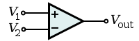
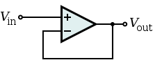
Compares two voltages and switches its output to indicate which voltage is larger.

(where is the supply voltage and the opamp is powered by and .)


Inverting amplifier
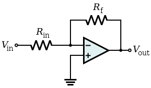
An inverting amplifier uses negative feedback to invert and amplify a voltage. The Rf resistor allows some of the output signal to be returned to the input. Since the output is 180° out of phase, this amount is effectively subtracted from the input, thereby reducing the input into the operational amplifier. This reduces the overall gain of the amplifier and is dubbed negative feedback.[1]

- (because is a virtual ground)
- A third resistor, of value , added between the non-inverting input and ground, while not necessary, minimizes errors due to input bias currents.[2]


The gain of the amplifier is determined by the ratio of Rf to Rin. That is:

The presence of the negative sign is a convention indicating that the output is inverted. For example, if Rf is 10 000 Ω and Rin is 1 000 Ω, then the gain would be -10 000Ω/1 000Ω, which is -10. [3]
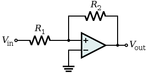
Non-inverting amplifier
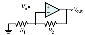
Amplifies a voltage (multiplies by a constant greater than 1)

- Input impedance
- The input impedance is at least the impedance between non-inverting () and inverting () inputs, which is typically 1 MΩ to 10 TΩ, plus the impedance of the path from the inverting () input to ground (i.e., in parallel with ).
- Because negative feedback ensures that the non-inverting and inverting inputs match, the input impedance is actually much higher.
- Although this circuit has a large input impedance, it suffers from error of input bias current.
- The non-inverting () and inverting () inputs draw small leakage currents into the operational amplifier.
- These input currents generate voltages that act like unmodeled input offsets. These unmodeled effects can lead to noise on the output (e.g., offsets or drift).
- Assuming that the two leaking currents are matched, their effect can be mitigated by ensuring the DC impedance looking out of each input is the same.
- The voltage produced by each bias current is equal to the product of the bias current with the equivalent DC impedance looking out of each input. Making those impedances equal makes the offset voltage at each input equal, and so the non-zero bias currents will have no impact on the difference between the two inputs.
- A resistor of value
- which is the equivalent resistance of in parallel with , between the source and the non-inverting () input will ensure the impedances looking out of each input will be matched.
- The matched bias currents will then generate matched offset voltages, and their effect will be hidden to the operational amplifier (which acts on the difference between its inputs) so long as the CMRR is good.
- Very often, the input currents are not matched.
- Most operational amplifiers provide some method of balancing the two input currents (e.g., by way of an external potentiometer).
- Alternatively, an external offset can be added to the operational amplifier input to nullify the effect.
- Another solution is to insert a variable resistor between the source and the non-inverting () input. The resistance can be tuned until the offset voltages at each input are matched.
- Operational amplifiers with MOSFET-based input stages have input currents that are so small that they often can be neglected.


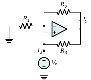
Differential amplifier
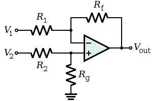
The circuit shown is used for finding the difference of two voltages each multiplied by some constant (determined by the resistors).
The name "differential amplifier" should not be confused with the "differentiator", also shown on this page.

- Differential (between the two input pins) = (Note: this is approximate)


For common-mode rejection, anything done to one input must be done to the other. The addition of a compensation capacitor in parallel with Rf, for instance, must be balanced by an equivalent capacitor in parallel with Rg.
The "instrumentation amplifier", which is also shown on this page, is another form of differential amplifier that also provides high input impedance.
Whenever and , the differential gain is


- and


When and the differential gain is A = 1 and the circuit acts as a differential follower:


Voltage follower
Used as a buffer amplifier to eliminate loading effects (e.g., connecting a device with a high source impedance to a device with a low input impedance).
- (realistically, the differential input impedance of the op-amp itself, 1 MΩ to 1 TΩ)


Due to the strong (i.e., unity gain) feedback and certain non-ideal characteristics of real operational amplifiers, this feedback system is prone to have poor stability margins. Consequently, the system may be unstable when connected to sufficiently capacitive loads. In these cases, a lag compensation network (e.g., connecting the load to the voltage follower through a resistor) can be used to restore stability. The manufacturer data sheet for the operational amplifier may provide guidance for the selection of components in external compensation networks. Alternatively, another operational amplifier can be chosen that has more appropriate internal compensation.
Summing amplifier
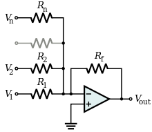
A summing amplifer sums several (weighted) voltages:

- When , and independent


- When


- Output is inverted
- Input impedance of the nth input is ( is a virtual ground)

Inverting integrator
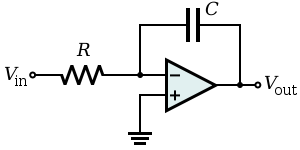
Integrates the (inverted) signal over time

(where and are functions of time, is the output voltage of the integrator at time t = 0.)


- Note that this can also be viewed as a low-pass electronic filter. It is a filter with a single pole at DC (i.e., where ) and gain.
- There are several potential problems with this circuit.
- It is usually assumed that the input has zero DC component (i.e., has a zero average value). Otherwise, unless the capacitor is periodically discharged, the output will drift outside of the operational amplifier's operating range.
- Even when has no offset, the leakage or bias currents into the operational amplifier inputs can add an unexpected offset voltage to that causes the output to drift. Balancing input currents and replacing the non-inverting () short-circuit to ground with a resistor with resistance can reduce the severity of this problem.
- Because this circuit provides no DC feedback (i.e., the capacitor appears like an open circuit to signals with ), the offset of the output may not agree with expectations (i.e., may be out of the designer's control with the present circuit).


- Many of these problems can be made less severe by adding a large resistor in parallel with the feedback capacitor. At significantly high frequencies, this resistor will have negligible effect. However, at low frequencies where there are drift and offset problems, the resistor provides the necessary feedback to hold the output steady at the correct value. In effect, this resistor reduces the DC gain of the "integrator" – it goes from infinite to some finite value .


Inverting differentiator
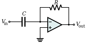
Differentiates the (inverted) signal over time.

- Note that this can also be viewed as a high-pass electronic filter. It is a filter with a single zero at DC (i.e., where ) and gain. The high pass characteristics of a differentiating amplifier can lead to unstable behavior when the circuit is used in an analog servo loop. For this reason the system function would be re-formulated to use integrators.
Instrumentation amplifier
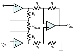
Combines very high input impedance, high common-mode rejection, low DC offset, and other properties used in making very accurate, low-noise measurements
- Is made by adding a non-inverting buffer to each input of the differential amplifier to increase the input impedance.
Schmitt trigger
A bistable multivibrator implemented as a comparator with hysteresis.
In this configuration, the input voltage is applied through the resistor (which may be the source internal resistance) to the non-inverting input and the inverting input is grounded or referenced. The hysteresis curve is non-inverting and the switching thresholds are where is the greatest output magnitude of the operational amplifier.


Alternatively, the input source and the ground may be swapped. Now the input voltage is applied directly to the inverting input and the non-inverting input is grounded or referenced. The hysteresis curve is inverting and the switching thresholds are . Such a configuration is used in the relaxation oscillator shown below.

Relaxation oscillator
By using an RC network to add slow negative feedback to the inverting Schmitt trigger, a relaxation oscillator is formed. The feedback through the RC network causes the Schmitt trigger output to oscillate in an endless symmetric square wave (i.e., the Schmitt trigger in this configuration is an astable multivibrator).
Inductance gyrator
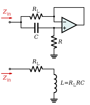
Simulates an inductor (i.e., provides inductance without the use of a possibly costly inductor). The circuit exploits the fact that the current flowing through a capacitor behaves through time as the voltage across an inductor. The capacitor used in this circuit is smaller than the inductor it simulates and its capacitance is less subject to changes in value due to environmental changes.
This circuit is unsuitable for applications relying on the back EMF property of an inductor as this will be limited in a gyrator circuit to the voltage supplies of the op-amp.
Zero level detector
Voltage divider reference
- Zener sets reference voltage.
- Acts as a comparator with one input tied to ground.
- When input is at zero, op-amp output is zero (assuming split supplies.)
Negative impedance converter (NIC)
Creates a resistor having a negative value for any signal generator
- In this case, the ratio between the input voltage and the input current (thus the input resistance) is given by:

In general, the components , , and need not be resistors; they can be any component that can be described with an impedance.

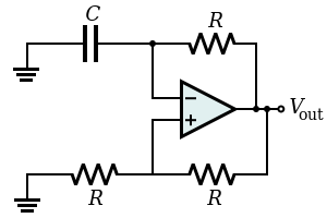
Wien bridge oscillator
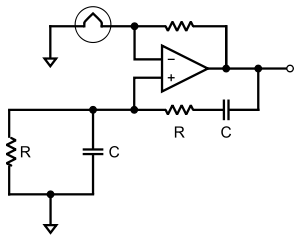
Produces a very low distortion sine wave. Uses negative temperature compensation in the form of a light bulb or diode.
Precision rectifier
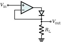
The voltage drop VF across the forward biased diode in the circuit of a passive rectifier is undesired. In this active version, the problem is solved by connecting the diode in the negative feedback loop. The op-amp compares the output voltage across the load with the input voltage and increases its own output voltage with the value of VF. As a result, the voltage drop VF is compensated and the circuit behaves very nearly as an ideal (super) diode with VF = 0 V.
The circuit has speed limitations at high frequency because of the slow negative feedback and due to the low slew rate of many non-ideal op-amps.
Logarithmic output
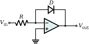
- The relationship between the input voltage and the output voltage is given by:


- where is the saturation current and is the thermal voltage.


- If the operational amplifier is considered ideal, the negative pin is virtually grounded, so the current flowing into the resistor from the source (and thus through the diode to the output, since the op-amp inputs draw no current) is:

- where is the current through the diode. As known, the relationship between the current and the voltage for a diode is:


- This, when the voltage is greater than zero, can be approximated by:

- Putting these two formulae together and considering that the output voltage is the negative of the voltage across the diode (), the relationship is proven.

Note that this implementation does not consider temperature stability and other non-ideal effects.
Exponential output
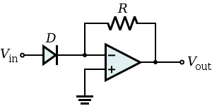
- The relationship between the input voltage and the output voltage is given by:

where is the saturation current and is the thermal voltage.
- Considering the operational amplifier ideal, then the negative pin is virtually grounded, so the current through the diode is given by:

when the voltage is greater than zero, it can be approximated by:
The output voltage is given by:

References
- ↑ Basic Electronics Theory, Delton T. Horn, 4th ed. McGraw-Hill Professional, 1994, p.342-343.
- ↑ Malmstadt, Enke and Crouch, Electronics and Instrumentation for Scientists, The Benjamin/Cummings Publishing Company, Inc., 1981, ISBN 0-8053-6917-1, Chapter 5. pp 118.
- ↑ Basic Electronics Theory, Delton T. Horn, 4th ed. McGraw-Hill Professional, 1994, p.342-343.